
For photographers and cinematographers, the image sensor is the heart of the modern camera—the digital equivalent of film stock. Every decision you make regarding exposure, lighting, dynamic range, and focus relies entirely on the capabilities and limitations of this silicon chip.
This comprehensive guide dives deep into the architecture, physics, and evolution of image sensors. By understanding the underlying mechanics—from the basic photodiode to advanced Dual Gain Output (DGO) and 2-Layer Transistor Pixels—you will be better equipped to choose the right gear and push your creative boundaries to their absolute limits.
Part 1: The Foundation of Digital Imaging
1. The Photodiode and the Photoelectric Effect
At the core of every digital image sensor is the photodiode, a semiconductor device that translates incoming light (photons) into an electrical current. When you press the shutter or hit record, light passes through your lens and strikes a vast grid of these photodiodes, each corresponding to a pixel in your final image.
Most camera sensors use silicon as their semiconductor material. In semiconductor physics, electrons sit in a "valence band" and require a minimum amount of energy—known as the band gap—to jump into the "conduction band" where they can flow as an electrical signal

For silicon, this band gap is 1.1 electron volts (eV). Visible light possesses more than enough energy to trigger this jump; for instance, a photon of red light carries about 2 eV, and blue light carries about 3 eV. When a photon strikes the silicon, its energy is absorbed, exciting an electron into the conduction band and leaving behind a "hole".
The photodiode operates in a state called "reverse bias," meaning an electric field is applied across it. This electric field causes the newly freed electron to be instantly swept toward the highest positive voltage in the pixel, where it is collected and measured as your image signal.
2. Anti-Reflective Coatings (ARC): Maximizing Light Capture
A major challenge in sensor design is that the silicon surface is highly reflective. If incident light bounces off the photodiode, that light is permanently lost, reducing the camera's quantum efficiency and responsivity.

To combat this, manufacturers apply an Anti-Reflective Coating (ARC), often made of materials like silicon nitride or silicon oxynitride, directly over the photodiode. The thickness of this coating is meticulously engineered to eliminate reflections at specific wavelengths. For visible light sensors, this layer is often between 470 and 830 angstroms thick. By minimizing reflection, ARC ensures that your camera gathers the maximum amount of light possible, resulting in a cleaner, more robust signal.
3. Dark Current and the Arrhenius Equation: The Enemy of Long Exposures
If you have ever shot a long exposure astrophotography image or recorded video in a hot environment, you have likely encountered thermal noise, also known as "dark current." Dark current is the generation of electron-hole pairs in the silicon without any light present.
This phenomenon is governed by the Arrhenius equation, a principle from statistical mechanics which states that as temperature increases, the reaction rate (in this case, the generation of unwanted electrons) increases exponentially. Dark current can be generated at the surface of the sensor or deep within the bulk of the silicon. For long-exposure photographers or cinema camera operators, this means that as your camera body heats up during operation, your sensor will inherently produce more noise, filling the shadows with grainy artifacts.
Part 2: The Great Divide: CCD vs. CMOS Architecture
The architecture used to read these captured electrons defines the overall performance of the camera. Historically, the industry was split between two monolithic architectures: CCD (Charge-Coupled Device) and CMOS (Complementary Metal-Oxide Semiconductor).
The CCD "Bucket Brigade"
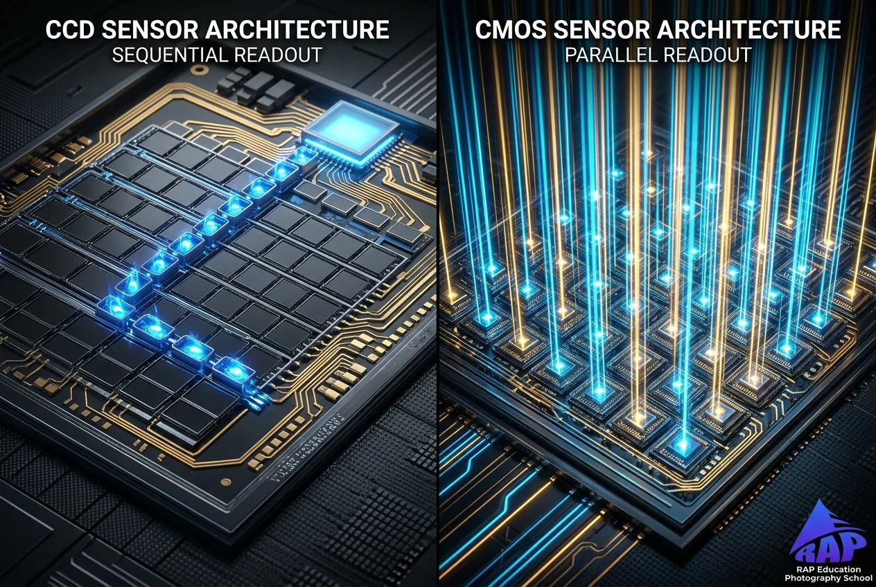
CCD sensors were the original standard for high-quality digital imaging. In a CCD sensor, once the exposure ends, the electrical charge from each pixel is shifted sequentially across the sensor array, moving from pixel to pixel until it reaches a single amplifier and an Analog-to-Digital Converter (ADC) at the edge of the chip.
Think of it as a bucket brigade: each pixel passes its "water" (electrons) to the next. Because the signal only passes through one or a few highly optimized amplifiers, CCDs traditionally offered incredibly low noise and high image uniformity. However, shuttling all that charge requires rapidly switching high voltages across the entire chip, meaning CCDs are notoriously power-hungry, prone to a visual artifact called "smearing," and suffer from slow readout speeds.
The CMOS Revolution
Starting around 2004, companies like Sony began heavily investing in CMOS technology. Unlike CCDs, a CMOS sensor features a dedicated amplifier (typically a source follower transistor) built directly into every single pixel.
Instead of passing the charge across the chip, a CMOS sensor converts the charge to a voltage right inside the pixel, and that voltage is read straight down a column to an ADC. Because each column can have its own ADC, CMOS sensors can be read out in parallel. This parallelism is what allows modern CMOS cameras to shoot 120 frames-per-second video and 30fps burst photography. CMOS sensors also require drastically less power. While early CMOS sensors suffered from higher noise (due to slight variations among the millions of individual pixel amplifiers), modern manufacturing and on-chip noise reduction have advanced to the point where CMOS image quality far surpasses that of legacy CCDs.
Part 3: Sensor Illumination and Architecture
Front-Side Illumination (FSI) vs. Back-Side Illumination (BSI)
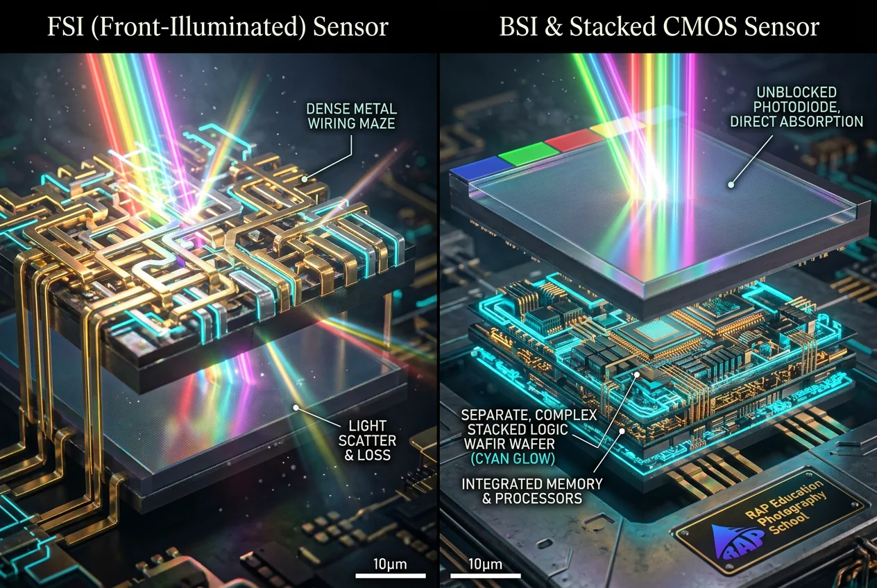
In traditional Front-Side Illuminated (FSI) CMOS sensors, the metal wiring used to control the pixels and carry the signal is placed on top of the silicon photodiode. When light enters the pixel, it must navigate past this maze of microscopic wires. If a photon hits the wiring, it is blocked or reflected, reducing light-gathering efficiency. Manufacturers historically mitigated this by applying "microlenses" above the pixels to funnel the light away from the wiring and into the photodiode.
However, the real breakthrough came with the Back-Side Illuminated (BSI) sensor. In a BSI sensor, the silicon wafer is flipped upside down, and the back is thinned out so that light enters the photodiode directly, with no metal wiring blocking the path. This essentially doubles the camera's sensitivity, fundamentally transforming low-light photography and enabling incredibly clean high-ISO performance.
The Stacked CMOS Sensor
In 2012, Sony pushed the envelope further with the "Stacked" CMOS sensor. Previously, the photodiode and the complex logic circuits (used for signal processing and autofocus) had to share space on the same layer of silicon. A stacked sensor separates these into two distinct chips: a pixel layer dedicated solely to gathering light, stacked directly on top of a logic chip containing the processing circuits. This allows for larger photodiodes (better dynamic range) and massive, high-speed logic circuits (enabling incredibly fast readout speeds and minimizing rolling shutter).
The Game Changer: 2-Layer Transistor Pixels
The most recent architectural revolution is the 2-Layer Transistor Pixel. In a conventional stacked sensor, the photodiode and the pixel transistors (the reset, select, and amplifier transistors necessary for the pixel to function) still share the same physical layer.
The 2-Layer Transistor Pixel uses proprietary technology to separate the photodiode onto one substrate and the pixel transistors onto another substrate beneath it. By removing the transistors from the top layer, the photodiode can be significantly enlarged, approximately doubling the "saturation signal level"—the maximum amount of light a pixel can hold before blowing out.
Simultaneously, the extra space on the transistor layer allows manufacturers to use much larger amplifier transistors. Larger amplifiers inherently generate less noise. For photographers and cinematographers, this technology achieves two massive feats simultaneously: it vastly widens the dynamic range (preventing blown highlights in backlit scenes) and drastically reduces shadow noise in dim, low-light environments, bringing the camera's capture closer to the perception of the naked human eye.
Part 4: Shutter Technologies—Capturing Motion
How an image sensor begins and ends its exposure defines how it renders motion. This is a critical consideration for sports photographers and cinematographers dealing with fast-moving action or rapid camera panning.
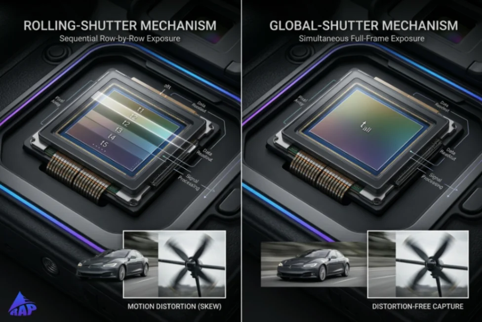
Rolling Shutter
The vast majority of modern CMOS sensors utilize a "rolling shutter." In this design, the sensor starts and stops its exposure line-by-line, sequentially from the top of the sensor to the bottom. Because the bottom of the image is exposed slightly later than the top, fast-moving objects or rapid camera pans result in a "jello effect" or skewed, leaning vertical lines.
However, rolling shutter sensors generally offer superior dynamic range and cleaner shadows compared to global shutters, making them excellent for static subjects, portraiture, and narrative cinema where camera movements are controlled. Advanced stacked sensors (such as those in the Canon EOS R1 and R5 Mark II) achieve extremely fast sensor readout speeds, reducing the rolling shutter distortion to almost imperceptible levels without sacrificing image quality.
Global Shutter
A global shutter starts and stops the exposure for every single pixel on the sensor simultaneously. CCDs inherently used global shutters, but bringing global shutters to CMOS sensors has been technically challenging. A global shutter completely eliminates the "jello effect," skewing, and flash banding, making it the holy grail for high-speed sports photography, action cinematography, and machine vision. However, global shutter CMOS architecture is complex, traditionally introduces slightly more image noise, and reduces the overall dynamic range.
Part 5: Specialized Sensor Tech for the Working Pro
Camera manufacturers have engineered highly specialized technologies to address specific needs in professional imaging:
1. Canon Dual Gain Output (DGO) for Cinematic HDR
Cinematographers constantly battle mixed lighting, such as shooting a subject in a dark room with bright sunlight streaming through a window. Canon's DGO technology (found in cameras like the Cinema EOS C300 Mark III and C70) addresses this at the hardware level.
A DGO sensor reads every single photodiode at two different amplification levels (gains) simultaneously. One readout uses high gain, prioritizing shadow details and minimizing noise; the other uses low gain to protect highlight information. The sensor then combines these two readouts on the fly to output a single image with astonishingly high dynamic range (up to 16 stops) and incredibly clean shadows. Crucially, because it is done in a single exposure, DGO does not consume extra power and completely avoids the motion artifacts associated with traditional multi-exposure HDR techniques.
2. Dual Pixel and Cross-Type Autofocus
Autofocus is no longer just a software feature; it is built into the sensor silicon. Canon's Dual Pixel CMOS AF splits every single pixel on the sensor into two separate photodiodes (A and B). By comparing the slight phase difference in the light hitting the left and right sides of the pixel, the sensor can instantly calculate the exact distance to the subject.
In 2024, Canon evolved this into Dual Pixel Intelligent AF with Cross-Type AF points (found in the EOS R1). Instead of just reading phase differences horizontally, the sensor's photodiodes are arranged to detect phase differences both horizontally and vertically simultaneously. This prevents the camera from losing focus on low-contrast subjects or subjects composed solely of horizontal lines, ensuring flawless tracking during high-speed sports or complex tracking shots.
3. SPAD (Single Photon Avalanche Diode) Sensors
For documentary filmmakers or surveillance operators working in near-total darkness, traditional CMOS and CCD sensors eventually fail because the electrical charge of a single photon is too small to overcome the sensor's base read noise.
Canon’s SPAD sensor utilizes a phenomenon called "Avalanche Multiplication." When a single photon strikes a SPAD sensor, it generates an electron, which is then accelerated to trigger a chain reaction—an avalanche—of up to one million electrons. This massive, instantaneous current pulse allows the camera to literally count individual photons. Cameras equipped with SPAD sensors, like the Canon MS-500, can capture full-color, high-definition video in environments that appear pitch-black to the naked eye.
4. Sony LOFIC and STARVIS Sensors
For highly unpredictable lighting—such as dashcams moving from dark tunnels into bright sunlight—Sony developed the STARVIS 3 sensor line incorporating LOFIC (Lateral OverFlow Integration Capacitor) technology. LOFIC acts as an overflow reservoir for electrons. When a pixel fills up and would normally clip (blow out the highlights), the excess charge bleeds into the LOFIC capacitor. This allows a single-shot exposure to achieve an enormous dynamic range (up to 96dB), maintaining perfectly exposed highlights and shadows without relying on multi-exposure HDR.
Part 6: Formats, Pixel Pitch, and Color Science
Sensor Formats and the Crop Factor
Image sensors are categorized by physical format, which profoundly affects the field of view, depth of field, and light-gathering capability.
- Full-Frame (36 x 24mm): The gold standard for professional portraiture, architecture, and high-end video. It provides a wide dynamic range, excellent low-light performance, and shallow depth of field.
- Super 35mm (approx. 24.6 x 13.8mm): The historic standard in the cinema industry. It balances cost, excellent cinematic image quality, and a manageable depth of field that allows focus pullers to do their jobs effectively.
- APS-C (22.2 x 14.8mm): Similar in size to Super 35, APS-C sensors impose a "crop factor" on full-frame lenses. On a Canon APS-C camera, a 1.6x crop factor means a 50mm lens provides the field of view of an 80mm lens. This "extended reach" makes APS-C sensors incredibly popular for wildlife, sports, and street photography.
Pixel Pitch: The "Light Bucket" Analogy
While a camera might boast 50 Megapixels, the physical size of those pixels (pixel pitch, measured in micrometers or µm) dictates light sensitivity. Think of a pixel as a "light bucket." If you compare a 21MP APS-C sensor to a 21MP Full-Frame sensor, the Full-Frame sensor has a significantly larger surface area, meaning each individual pixel (bucket) is wider. A wider bucket catches more "rain" (photons) with relatively less random electronic noise. Therefore, if two sensors share the same resolution, the one with the larger physical footprint will inherently perform better in low light.
Monochrome vs. Color: The Bayer Filter
By nature, silicon photodiodes are monochromatic; they only measure the intensity of light, not its color. To produce a color image, manufacturers place a microscopic mosaic of color filters over the pixels.
The most common arrangement is the Bayer filter, which consists of a repeating grid of 50% Green, 25% Red, and 25% Blue filters. (There is more green because the human eye is most sensitive to green wavelengths). Because each pixel only records one color, the camera’s image processor must perform a complex mathematical process called "demosaicing" or "debayering" to interpolate the missing color data from neighboring pixels.
Dedicated monochromatic cinema sensors omit this color filter entirely. Without the filter absorbing incoming light, every single pixel receives the full spectrum of visible light. This is why native monochrome cameras exhibit sharper details and superior low-light sensitivity (quantum efficiency) compared to their color counterparts.
Conclusion: Mastering Your Medium
The image sensor is a marvel of quantum physics and microscopic engineering. Every advancement—from separating photodiode layers to multiplying single photons in an avalanche—has been driven by the need to conquer darkness, preserve highlights, and capture motion with absolute fidelity.
As a photographer or cinematographer, understanding these mechanics demystifies the behavior of your camera. You now know why your camera produces noise when it overheats during a long take, why a stacked sensor saves you from the "jello effect" on a fast pan, and why a dual-gain architecture allows you to confidently expose for the shadows without losing the sky. Armed with this knowledge, you are no longer just operating a piece of consumer electronics; you are wielding a highly tuned optical instrument capable of transforming the photons of the physical world into your creative vision.
- #Digital image sensor
- #Photodiode physics
- #Anti-Reflective Coating (ARC)
- #Back-Side Illumination (BSI)
- #Stacked CMOS architecture
- #Global shutter